-
Product Categories
Live Support Chat


Clone IC AT89C51ED2 Code
Clone IC AT89C51ED2 Code from AT89C51ED2 embedded flash memory, the extracted heximal from IC chip will be exactly the same as original MCU after recovery;
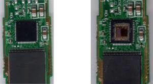
Clone IC AT89C51ED2 Code from AT89C51ED2 embedded flash memory, the extracted heximal from IC chip will be exactly the same as original MCU after recovery
The AT89C51RD2/ED2 core needs only 6 clock periods per machine cycle. This feature called ‘X2’ provides the following advantages:
Divide frequency crystals by 2 (cheaper crystals) while keeping same CPU power. Save power consumption while keeping same CPU power (oscillator power saving). Save power consumption by dividing dynamically the operating frequency by 2 in operating and idle modes.
Increase CPU power by 2 while keeping same crystal frequency. In order to keep the original C51 compatibility, a divider by 2 is inserted between the XTAL1 signal and the main clock input of the core (phase generator). This divider may be disabled by software if microcontroller pic18f1230 code extraction.
The clock for the whole circuit and peripherals is first divided by two before being used by the CPU core and the peripherals. This allows any cyclic ratio to be accepted on XTAL1 input. In X2 mode, as this divider is bypassed, the signals on XTAL1 must have a cyclic ratio between 40 to 60%.
Figure 5 shows the clock generation block diagram. X2 bit is validated on the rising edge of the XTAL1 ÷ 2 to avoid glitches when switching from X2 to STD mode. Figure 6 shows the switching mode waveforms. The X2 bit in the CKCON0 register (see Table 16) allows a switch from 12 clock periods per instruction to 6 clock periods and vice versa. At reset, the speed is set according to X2 bit of Hardware Security Byte (HSB). By default, Standard mode is active. Setting the X2 bit activates the X2 feature (X2 mode) after PIC18F2220 IC software unlocking.
The T0X2, T1X2, T2X2, UartX2, PcaX2, and WdX2 bits in the CKCON0 register (Table 16) and SPIX2 bit in the CKCON1 register (see Table 17) allows a switch from standard peripheral speed (12 clock periods per peripheral clock cycle) to fast peripheral speed (6 clock periods per peripheral clock cycle). These bits are active only in X2 mode.
As detailed in Section “Hardware Watchdog Timer”, page 86, the WDT generates a 96- clock period pulse on the RST pin. In order to properly propagate this pulse to the rest of the application in case of external capacitor or power-supply supervisor circuit, a 1 kΩ resistor must be added.
The POR/PFD function monitors the internal power-supply of the CPU core memories and the peripherals, and if needed, suspends their activity when the internal power supply falls below a safety threshold. This is achieved by applying an internal reset to them.
By gen erating the Re se t the Power Monito r insures a correct start up whe n AT89C51RD2/ED2 is powered up.
In order to startup and maintain the microcontroller in correct operating mode, VCC has to be stabilized in the VCC operating range and the oscillator has to be stabilized with a nominal amplitude compatible with logic level VIH/VIL. These parameters are controlled during the three phases: power-up, normal operation and power going down. See Figure 12.
When the power is applied, the Power Monitor immediately asserts a reset. Once the internal supply after the voltage regulator reach a safety level, the power monitor then looks at the XTAL clock input. The internal reset will remain asserted until the Xtal1 levels are above and below VIH and VIL. Further more. An internal counter will count 1024 clock periods before the reset is de-asserted when Clone IC AT89C51ED2 Code.
If the internal power supply falls below a safety level, a reset is immediately asserted.
Tags: Clone IC flash archive,Clone IC flash code,Clone IC flash content,Clone IC flash data,Clone IC flash eeprom,Clone IC flash file,Clone IC flash firmware,Clone IC flash information,Clone IC flash memory,Clone IC flash program


