-
Product Categories
Live Support Chat


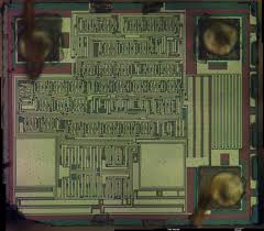
Break Microchip IC PIC16F631 Heximal
Break Microchip IC PIC16F631 needs to break mcu pic16f631 flash memory fuse bit by focus ion beam and extract embedded code from microcontroller pic16f631;
Program Memory Organization
The PIC12F631 has a 13-bit program counter capable of addressing an 8k x 14 program memory space. Only the first 2k x 14 (0000h-07FFh) for the PIC12F631 is physically implemented. Accessing a location above these boundaries will cause a wraparound within the first 2K x 14 space. The Reset vector is at 0000h and the interrupt vector is at 0004h.
DATA MEMORY ORGANIZATION
The data memory is partitioned into two banks, which contain the General Purpose Registers (GPR) and the Special Function Registers (SFR). The Special Function Registers are located in the first 32 locations of each bank. Register locations 20h-7Fh in Bank 0 and A0h-BFh in Bank 1 are General Purpose Registers, implemented as static RAM. Register locations F0h-FFh in Bank 1 point to addresses 70h-7Fh in Bank 0. All other RAM is unimplemented and returns ‘0’ when read. RP0 of the STATUS register is the bank select bit if unlock atmega48a mcu flash.
Special FUNCTIONS REGISTER
The Special Function Registers are registers used by the CPU and peripheral functions for controlling the desired operation of the device. These registers are static RAM.
The special registers can be classified into two sets: core and peripheral. The Special Function Registers associated with the “core” are described in this section. Those related to the operation of the peripheral features are described in the section of that peripheral feature.
STATUS REGISTER
The STATUS register, shown in Register 2-1, contains:
· Arithmetic status of the ALU
· Reset status
· Bank select bits for data memory (SRAM)
The STATUS register can be the destination for any instruction, like any other register. If the STATUS register is the destination for an instruction that affects the Z, DC or C bits, then the write to these three bits is disabled. These bits are set or cleared according to the device logic. Furthermore, the TO and PD bits are not writable. Therefore, the result of an instruction with the STATUS register as destination may be different than intended for the purpose of break Microchip IC.