-
Product Categories
Live Support Chat


Attack Microcontroller PIC16F767 Program
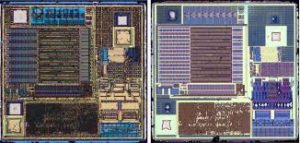
Attack Microcontroller PIC16F767 protective system and disable its tamper resistance, recover Program from mcu flash memory and download the code to blank PIC16F767 microprocessor;
Attack Microcontroller PIC16F767 protective system and disable its tamper resistance, recover Program from mcu flash memory and download the code to blank PIC16F767 microprocessor
MEMORY ORGANIZATION
There are two memory blocks in each of these PICmicro® MCUs. The program memory and data memory have separate buses so that concurrent access can occur and is detailed in this section. The program memory can be read internally by user code (see Section 3.0 “Reading Program Memory”) when attack microcontroller.
Additional information on device memory may be found in the “PICmicro® Mid-Range MCU Family Reference Manual” (DS33023).
The PIC16F767 devices have a 13-bit program counter capable of addressing an 8K word x 14-bit program memory space. The PIC16F767 devices have 8K words of Flash program memory and the PIC16F767 devices have 4K words. The program memory maps for PIC16F7X7 devices are shown in Figure 2-1. Accessing a location above the physically implemented address will cause a wraparound. in the “PICmicro® Mid-Range MCU Family Reference.
The Reset vector is at 0000h and the interrupt vector is at 0004h after mcu pic16f676 code extraction.
The data memory is partitioned into multiple banks which contain the General Purpose Registers and the Special Function Registers. Bits RP1 (Status<6>) and RP0 (Status<5>) are the bank select bits if microcontroller pic16f747 code extraction:
|
RP1:RP0 |
Bank |
|
00 |
0 |
|
01 |
1 |
|
10 |
2 |
|
11 |
3 |
Each bank extends up to 7Fh (128 bytes). The lower locations of each bank are reserved for the Special Function Registers. Above the Special Function Registers are General Purpose Registers, implemented as static RAM. All implemented banks contain Special Function Registers. Some frequently used Special Function Registers from one bank may be mirrored in another bank for code reduction and quicker access.